- LTL in Etcheverry Hall
- UC Berkeley Campus
- LBNL
LTL in Etcheverry HallLocation and Workspace
Total working area: 2,000 sq. ft.
- Offices (#5144, #5216, at Etcheverry Hall) - Lab. (#5115, #6116, #6162, #6186, at Etcheverry Hall) |

|
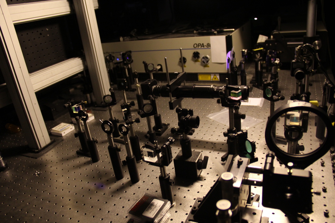
Lasers
|


|
Nano-particle synthesis and Patterning Stages
|
|
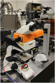
Characterization and Imaging System
|
(a) Gated ICCD camera, <2 ns minimum gate width
(b) Imaging Spectrograph and Monochromator (c) Veeco Atomic force microscope (AFM) (d) Near-field Scanning Optical Misroscopes (NSOMs) from Nanonics and Park Systems (e) Semiconductor analyzer (f) Solar cell simulator (g) A John Woolam Co. VASE scanning ellipsometer (h) A Renishaw inVia Basis Raman system |
|
For a complete list of facilities, please download:
| ltl_facility_kwon.docx |
UC Berkeley Campus

|
Marvell Nanolab
The Marvell NanoLab, located in the CITRIS headquarters building, Sutardja Dai Hall , includes more than 15,000 sq feet of Class100 and Class1000 cleanroom. The Marvell NanoLab is a shared research center providing more than 100 Principal Investigators and over 500 academic and industrial researchers a complete set of micro- and nano-fabrication tools. |

|
Bimolecular Nanotechnology Center
is an 11,500 sq ft class 1,000/10,000 cleanroom facility located in Stanley Hall on the UC Berkeley campus. The BNC is a unique fabrication and experimentation facility specializing in BioMEMS (Biomedical Micro-electromechanical systems) and Microfluidic devices. The center focuses on microfluidic processing of glass and polymer materials. Experimentation on proteins, nucleic acids, cells, and tissues are encouraged. In addition to a state-of-the-art research lab, the center also features a teaching lab for hands-on training of both undergraduate and graduate students.
|

|
The Berkeley Sensor & Actuator Center (BSAC):
- The National Science Foundation Industry/University Cooperative Research Center for Microsensors and Microactuators, conducts industry-relevant, interdisciplinary research on micro- and nano-scale sensors, moving mechanical elements, microfluidics, materials, and processes that take advantage of progress made in integrated-circuit, bio, and polymer technologies |
Lawrence Berkeley National Lab

|
National Center for Electron Microscopy
NCEM is a Department of Energy (DOE) sponsored user facility for electron beam microcharacterization. Equipment include the JEOL 3011 in situ TEM, the Zeiss Libra 200kV FEG TEM and the FEI dual-beam Strata 235 FIB. NCEM currently operates 8 dedicated Transmission Electron Microscopes. The available microscopes cover a wide range of state-of-the-art or unique capabilities, among them instruments that are specialized for high resolution, analytical, soft materials, and in situ experiments. Through the TEAM project (Transmission Electron Aberration-corrected Microscope) two new aberration-corrected microscopes have been installed at NCEM. TEAM 0.5, is a double-Cs corrected FEI Titan STEM/TEM and TEAM I is the world’s first Cs and Cc corrected electron microscope. |

|
The Advanced Light Source (ALS)
As a division of Berkeley Lab, ALS is a national user facility that generates intense light for scientific and technological research. As one of the world's brightest sources of ultraviolet and soft x-ray beams--and the world's first third-generation synchrotron light source in its energy range--the ALS makes previously impossible studies possible. The facility welcomes researchers from universities, industries, and government laboratories around the world. |

|
The Molecular Foundry
The Molecular Foundry is a User Facility charged with providing support to nanoscience researchers in academic, government and industrial laboratories around the world. The Foundry provides users with instruments, techniques and collaborators to enhance their studies of the synthesis, characterization and theory of nanoscale materials. Its six facilities focus on both “soft” (biological and polymeric) and “hard” (inorganic and microfabricated) nanostructured building blocks, and their integration into complex functional assemblies. Users are invited to submit proposals requesting free access to Foundry instruments, techniques, and skilled staff. |